History
Nanotronix has developed various 2D/3D fine patterning using glass as a substrate, and has experience in developing both TSV and TGV through-hole electrodes.
Currently, we are focusing on developing plating total solution (pretreatment, seed & fill) for TGV metallization of large glass substrates.
-
2009TSV metallization(seed plating)
- - >Ø 10µm
- - Process tools development
-
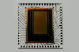
2015CIS pan-out @ glass
- - Sputter seed base
- - Build-up Plating
-
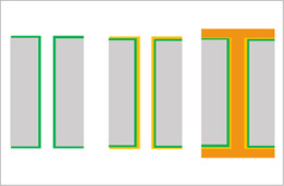
2019micro-LED TFT edge patterns (ink. Embedded : > 20µm)

-
2022 Glass PCB (signage, etc.)
Direct patterning on the glass for outdoor signage
-
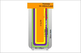
2022~TGV metallization(seed plating)
- - Adhesive layer
- - Seed layer(Ni/Cu)
- - All layers by plating process