TGV metallization
Nanotronix has been launching overseas plating technology in Korea since 2009, TSV(Through SIlicon Via), and has abundant experience in materials and equipment.
In particular, regarding glass substrates, we have been steadily developing TGV(Through Glass Via), which is attracting attention as a glass substrate technology for semiconductor(advanced packaging), and as a result, we completed the development of plating chemicals in 2024.
Currently, in the TGV structure possible with glass processing technology(diameter 10~100micro, thickness less than 1mm), a seed layer with an AR(Aspect Ratio) of 10~20 is possible through plating, and high-difficulty plating technology is implemented with conformal coating(step coverage 70% or more).
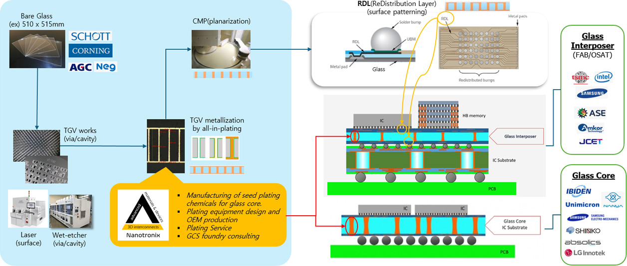
Nanotronix positioning in the supply chain of GIS & GCS as an IC substrate
Class Core performance
| Items | Adhesive layer(Via wall) | Seed layer | Fill | Summary |
|---|---|---|---|---|
| Thin Films | Ensuring adhesion between glass wall and metal layer | Securing adhesion between adhesive layer and Cu layer | Cu filling | |
| Major plating composition & performance |
Ni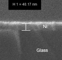
|
Cu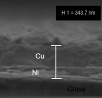
|
Cu : Full fill @ via 30um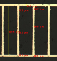
|
|
| Methods | Electro-less plating | Electro plating | Electro plating |