Sytem engineering
Nanotronix is applying various knowhow & technologies accumulated in semiconductors and displays to glass substrates, which is to broadly summarized as glass processing technology, glass patterning technology, metrology and power technology.
System engineering for Glass Core Substrate
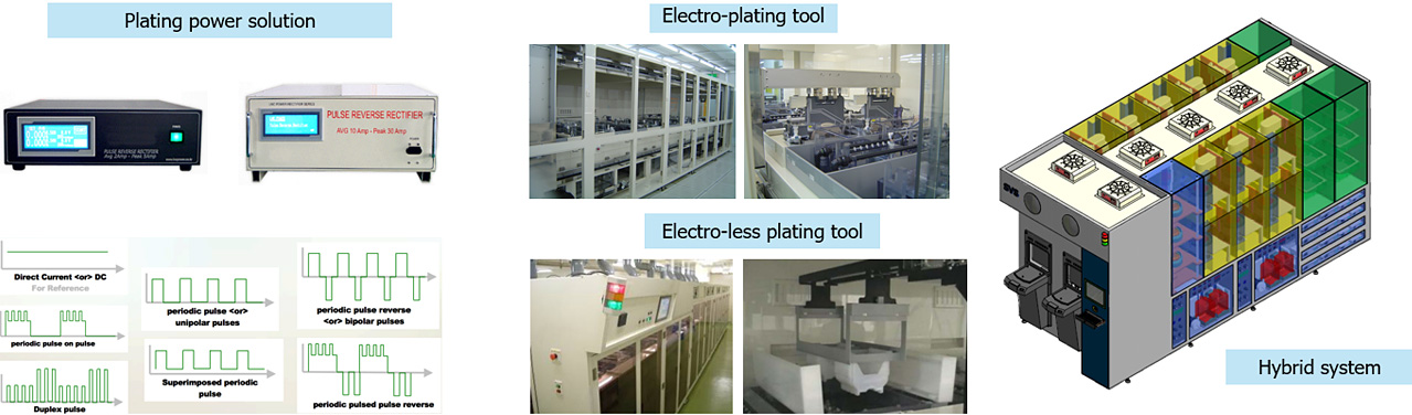
Nanotronix is developing equipment that can process electroless and electro-plating in batches based on the seed layer process technology for TGV metallization.
In particular, we are manufacturing power supplies, which are one of the core technologies for electroplating, and are also developing jigs and modules required for various plating processes.
System development for the advanced & new process
Nanotronix is continuously developing various process technologies and systems required for glass substrates, such as grooving, dicing, chamfering, and wet etching, with related partners, and also includes various measuring equipment required for glass processing and patterning.
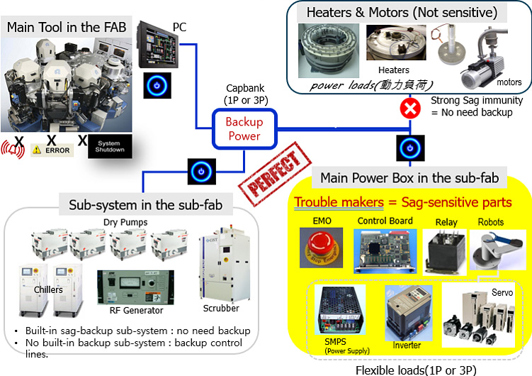
On the other hand, it supplies power backup systems with the concept of power vaccine for line stabilization to semiconductor IC fabs, OSAT, and display processes, and is also applied to glass substrate processes.
- Substrate machining system
- - Wafer/glass grooving and dicing by laser
- - Glass chamfering
- - Glass wet treatment(etching, healing, etc.)
- Metrology
- - 3D transparent substrate(TGV)
- - 3D interconnects(GCS) : surface(2D), via(3D)
- - Wafer/glass sensor
- Power solution for process tools(worldwide) : IC/Panel fabs, OSAT, Automotive
- - Power vaccine solution for all process tools(individual) : 1 sec backup under blackout
- - Better solution than SEMI-F47
- - Cap-bank base